Mizzou Engineers have come up with a novel new technique to design semiconductors, the chips that make your phones, laptops and other devices not only smart, but also compact.
“It’s not practical yet, but we want to take the underlying mechanism and make it scalable and something attractive to the semiconductor industry,” said Maschmann, an associate professor of mechanical and aerospace engineering.
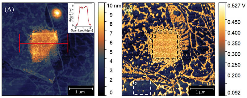
Semiconductors are made of layers of thin films, each of which are deposited or etched with specific patterns that impact their functions. Aligning patterns between processing steps makes the manufacturing process especially complex. The new process invented by Young and Maschmann is a different type of a technique known as area-selective atomic layer deposition (AS-ALD).
“To make these microchips, you need to control matter at the nanoscale; you need to control where atoms are positioned and where material is on a scale that’s a thousand times smaller than a human hair,” said Young, an assistant professor in biomedical, biological and chemical engineering. “For faster computers, you need to control matter on a smaller scale, approaching the size of an atom.”
Right now, AS-ALD occurs using self-assembled monolayers to block deposition of material in areas where it is not desired. Essentially, a liquid is spread onto a silicon wafer shaped with the desired pattern. Similar to a stencil, that allows the liquid to cover specific spaces without covering undesired areas.
Young and Maschmann have taken the opposite approach. They’re using an electron beam as a “pencil” to write the patterns exactly where they want them.
And they’re doing that work in a low-pressure water vapor, dissociating water molecules in collisions with the electron beam. One byproduct of the reaction is hydroxyl molecular groups, the initial layer of chemical functionalization needed for atomic layer deposition.
“It’s not a common environment to have — water vapor and focused electron beams,” Maschmann said.
That’s the beauty of the work, said Young, who has a joint appointment in chemistry. It ties his team’s expertise around atomic layer deposition together with Maschmann’s work with carbon nanomaterials and using electron microscopes in new ways.
The research is under the umbrella of the MU Materials Science & Engineering Institute (MUMSEI), which opened this past year to promote interdisciplinary work.
“This is exactly what we wanted to happen within the Institute,” Maschmann, a co-director of MUMSEI, said. “When you share space, you start to find shared interests that maybe weren’t apparent before. We were able to take advantage of that.”
Moving forward, the team will take advantage of resources at Mizzou’s Electron Microscopy Core to advance the project.